Technology

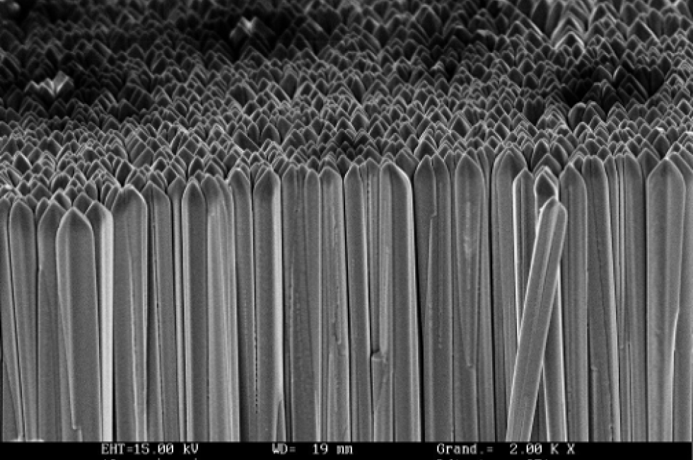
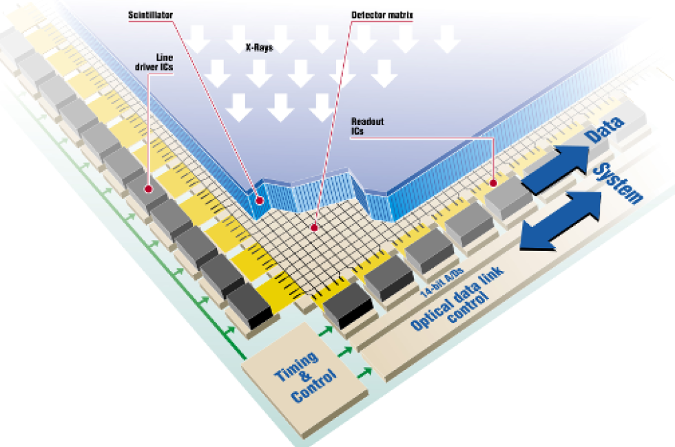
The principle of Trixell's flat panel detectors consists of a matrix of photodiodes made from amorphous silicon, covered with a cesium iodide scintillator.

X-rays are absorbed in the CsI layer and are converted into visible photons, which in turn generate electric charges in the photodiodes. Each pixel of the matrix is connected to a row line for driving voltages, and a column line for readout via an active switching element, which may be either a thin-film diode or a thin-film transistor. Electric charges are read out in parallel for one row. Signals are then multiplexed and converted digitally inside the detector housing. The data are transmitted to the acquisition system, where digital processing is performed.

panel detectors are based on proven core technologies:
• a cesium iodide scintillator (CsI)
• an active amorphous silicon array controlled by custom-designed, ultra-low noise electronics
  • Scintillator

    A scintillator layer to convert the incoming X-rays into visible light

    A scintillator is necessary for high-performance solid-state X-ray detectors.

    An overlying X-ray converter transforms X-ray photons into visible light which is detected by the photodiodes.

    Trixell uses a layer of cesium iodide doped with thallium Csl (TI) as an X-ray converter. This material provides high resolution and a high-absorption coefficient thanks to its needle (fiber optic-like) structure. This structure also limits the lateral diffusion light, further improving the resolution.

    With an excellent detectivity, from 40 kVp up to the highest kVp value, the cesium iodide is optimized for all radiographic applications.

  • Detector Matrix

    a-Si:H detector matrix sensitive to visible light

    These sensors typically consist of a 2D array. The photosensitive element in each pixel is an amorphous hydrogenated silicon (aSi:H) photodiode. The a-Si:H semi-conductor material is a very good photo detector in thin-film form (< 2µm), easy to deposit on large glass substrates.

    The light striking each photodiode generates a current which is integrated in the device's self-capacitance. The photo charge level is subsequently transferred to the external drive electronics by a matrix of a-Si:H switching devices.

    a-Si:H is very sensitive to visible light, with an efficiency close to 100% and a low dark current allowing highly sensitive image pick-up and low pixel noise.
     

    Amorphous silicon matrix:

    • The industry standard in large area electronics (liquid crystal displays)
    • Coupled with Cesium Iodide, the most effective way to obtain images for both radiography and fluoroscopy
    • High resolution over a large area
    • High efficiency for photon absorption
    • High stability relative to X-ray radiation
  • Drive Ics & Readout Ics

    Peripheral drive electronics: advanced, compact, low noise, low power ASICS and VLSI.

    Silicon integrated circuits are connected along the edges of the detector matrix, which provide the line scanning sequence, the signal readout amplification and the multiplexing.

    The design of the readout amplifier is key to the electronic noise performance of the detector. The readout amplifier is optimized to reduce the electronic noise below the signal given by one X-ray quanta.

    This low noise level, combined with high sensitivity, makes this component ideal for fluoroscopy applications.
     

    Custom electronics:

    • Ultra low noise custom designed readout amplifiers to obtain a high signal-to-noise ratio
    • Custom line drivers and low power readout amplifiers / multiplexers for fast and efficient reading
    • High performance electronics allow fast image acquisition:
      • Excellent image quality superior to film and CR
      • Immediate availability of the image